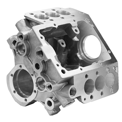









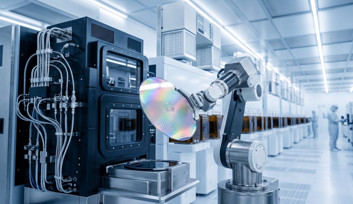
Semiconductor CNC Machining for Wafer Tools
Semiconductor CNC machining of chamber parts, wafer chucks, gas manifolds and showerheads to ±0.005 mm, finished to Ra 0.2–0.4 µm. Every part is cleaned and double-bagged particle-free.
-
ISO 9001

-
AS9100D

Semiconductor Equipment Parts Manufacturing at DEK
We machine parts for the tools that etch, deposit, clean, handle and inspect wafers, in 6061 and 7075 aluminum, 316L stainless, Kovar, Invar, titanium, PEEK and PTFE. Standard tolerance is ±0.005 mm, with finishes to Ra 0.2–0.4 µm where the drawing demands it.
An engineer reviews every drawing before quoting, usually within 6 hours. There is no minimum order, prototypes ship in 3–5 days, and parts are cleaned and packed particle-free. See our industries overview for the other sectors we supply.
Failure Modes We Design Out
- Particles shed from burrs and sharp edges on wafer-contact features
- Outgassing and virtual leaks from unvented blind holes in vacuum hardware
- Leaks at O-ring grooves with radial scratches or rough sealing faces
- Thermal drift and flatness loss on chucks, plates and metrology bases
-
0.005mm
Standard Metal Tolerance
-
0.2µm
Ra on Polished Faces
-
6h
Typical Quote Turnaround
-
2,300+
Customers Supplied
Components We Machine for Semiconductor Equipment
Each part family has its own failure mode: particles, outgassing, leaks, thermal drift or wafer damage. We machine around all of them.
-
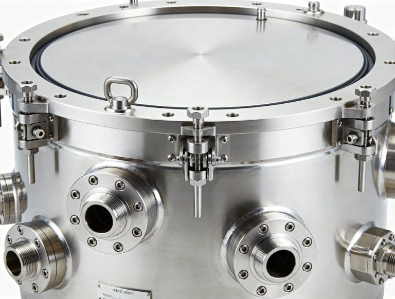
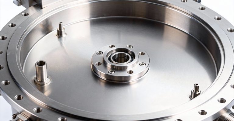 Vacuum Chamber ComponentsVacuum chamber components machining of lids, liners, pumping plates and viewport flanges with leak-tight O-ring grooves.
-
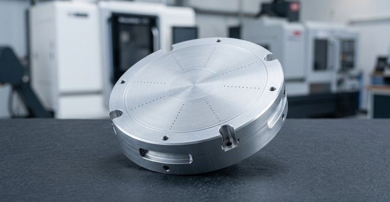 Wafer Chucks and PedestalsWafer chuck machining of vacuum and electrostatic chuck bodies, heater and lift-pin plates, ground and lapped flat.
-
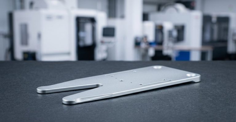 End EffectorsBlades, paddles and edge-grip fingers with thin sections held flat and burr-free so they never scratch a wafer.
-
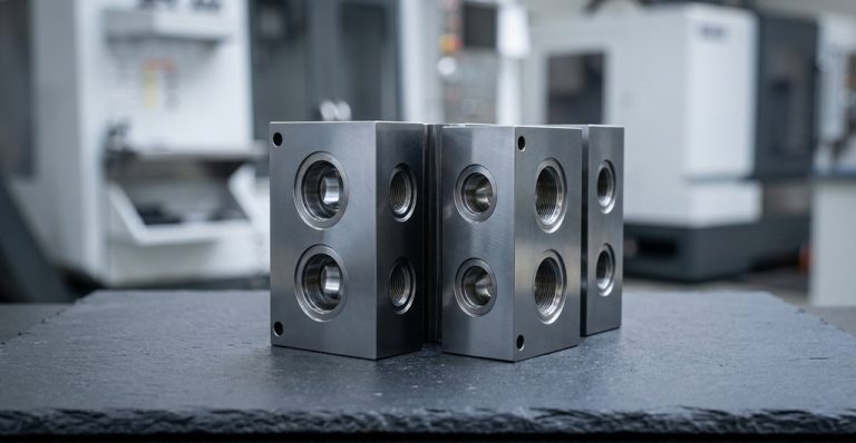 Gas Manifolds and Panel Blocks316L blocks with intersecting galleries, VCR-compatible face-seal ports and internal finishes suited to electropolishing.
-
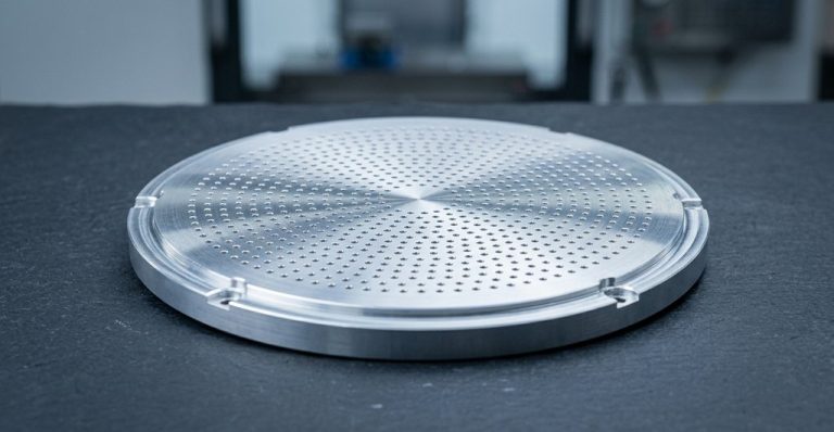 Showerheads and DiffusersAluminum or stainless plates with hundreds to thousands of 0.3–1.0 mm holes drilled at ±0.02 mm position.
-
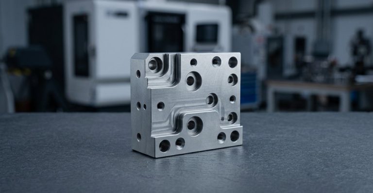 Fixtures and Metrology HardwareKovar and Invar bases where thermal expansion must stay near zero, plus aluminum tooling for probe stations.
-
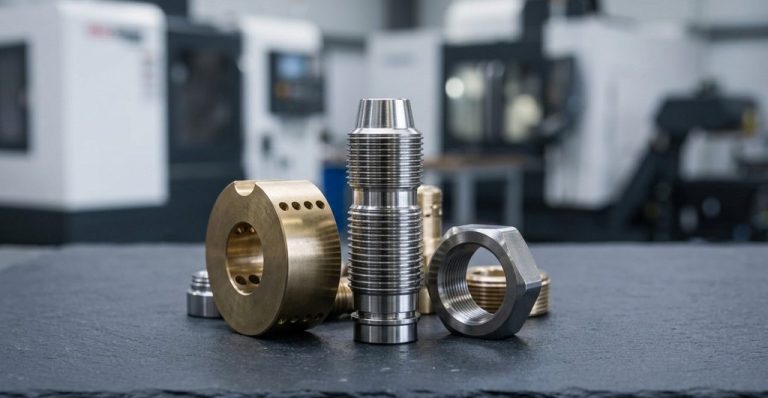 Ultra High Purity FittingsFace-seal glands, adapters and weld stubs in 316L with internal finishes to Ra 0.25 µm or better for gas delivery.


Semiconductor CNC Machining Capabilities
Cleanliness, tolerances, documentation and lifecycle support for semiconductor parts, planned from the drawing note to the packed bag.
Materials for Vacuum, Plasma and Cleanroom Use
Metals and polymers are our core semiconductor machining scope; choose by environment: vacuum, plasma, wet chemistry or thermal stability.
| Material | Where it is used | Machining notes |
|---|---|---|
| 6061 aluminum | Chamber lids, chuck bodies, end effectors | Machines fast; Type III hard anodize for plasma |
| 7075 aluminum | Robot arms, load-bearing brackets | Higher strength; watch thin-wall finishing |
| 316L stainless | Gas manifolds, UHP fittings, chamber hardware | Low-sulfur for electropolish; passivate after |
| Kovar | Glass-to-metal seals, feedthroughs, sensors | Gummy; sharp tools, rigid fixturing, ±0.005 mm |
| Invar | Metrology frames, optical mounts, stages | Low expansion; staged roughing and finishing |
| Titanium | Wet-bench hardware, corrosive-gas chamber parts | Low conductivity; slow, positive cutting |
| PEEK | End-effector pads, wafer carriers, insulators | Low outgassing; annealed stock stays flat |
| PTFE | Wet-process fittings, seals, chemical delivery | Creeps under load; ±0.05 mm typical |
| Ultem (PEI) | Test sockets, handler parts, insulators | Stable to 170 °C; ±0.01 mm on small features |
| PPSU | Steam- and chemical-exposed handling parts | Tough, autoclavable, machines like PC |
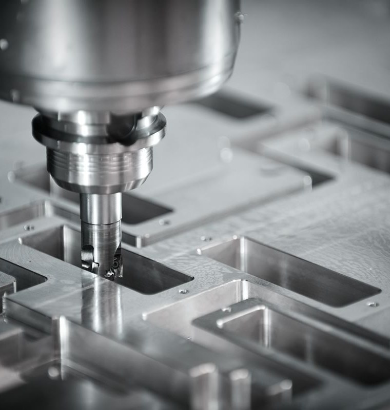
Why DEK for Semiconductor CNC Machining
Semiconductor work depends on details an automated quoting tool misses, so an engineer reads each drawing and prices the real route.
-

Machining Since 2002
Precision machining since 2002, with more than 2,300 customers in equipment, electronics and instrumentation relying on our parts.
-

TÜV-Certified Quality
ISO 9001:2015 and AS9100D certificates issued by TÜV cover the quality system behind every semiconductor order we ship.
-

Engineer-Reviewed Routes
We decide whether a 0.4 µm bore needs honing or polishing, whether Kovar will move, and whether anodizing needs masking.
-

Eight-Inspector QC Team
Eight inspectors, each with 5+ years' experience in European and American export standards, sign off every shipment.
Our Ordering Process
Semiconductor Materials and Finishes
Pair the right metal or polymer with the finish your chamber, gas line or handling part needs, all machined in-house.
Surface Finishes
Engineering Plastics
Need another alloy or finish? Ask our engineers to review it.
All MaterialsSemiconductor Machining FAQ
Common questions from semiconductor equipment buyers and engineers.
Request a Quote for Semiconductor Parts
Send your drawings with material, finish, cleanliness and packaging notes and the quantity per phase. An engineer reviews every file before quoting.
- PDF, STEP, IGES or SLDPRT accepted
- Quote within 6 hours for standard parts
- Up to 3 days for complex chamber assemblies
- No minimum order quantity
- Email quote@dekmake.com or use the form

Ready to Scale Your Project?
Get started with a stable process and controlled quality. Let's discuss your project.